Taiwan is mobilising its chipmaking sector to commercialise silicon photonics and copackaged optics, with the Ministry of Economic Affairs backing efforts to overcome artificial intelligence computing bottlenecks.
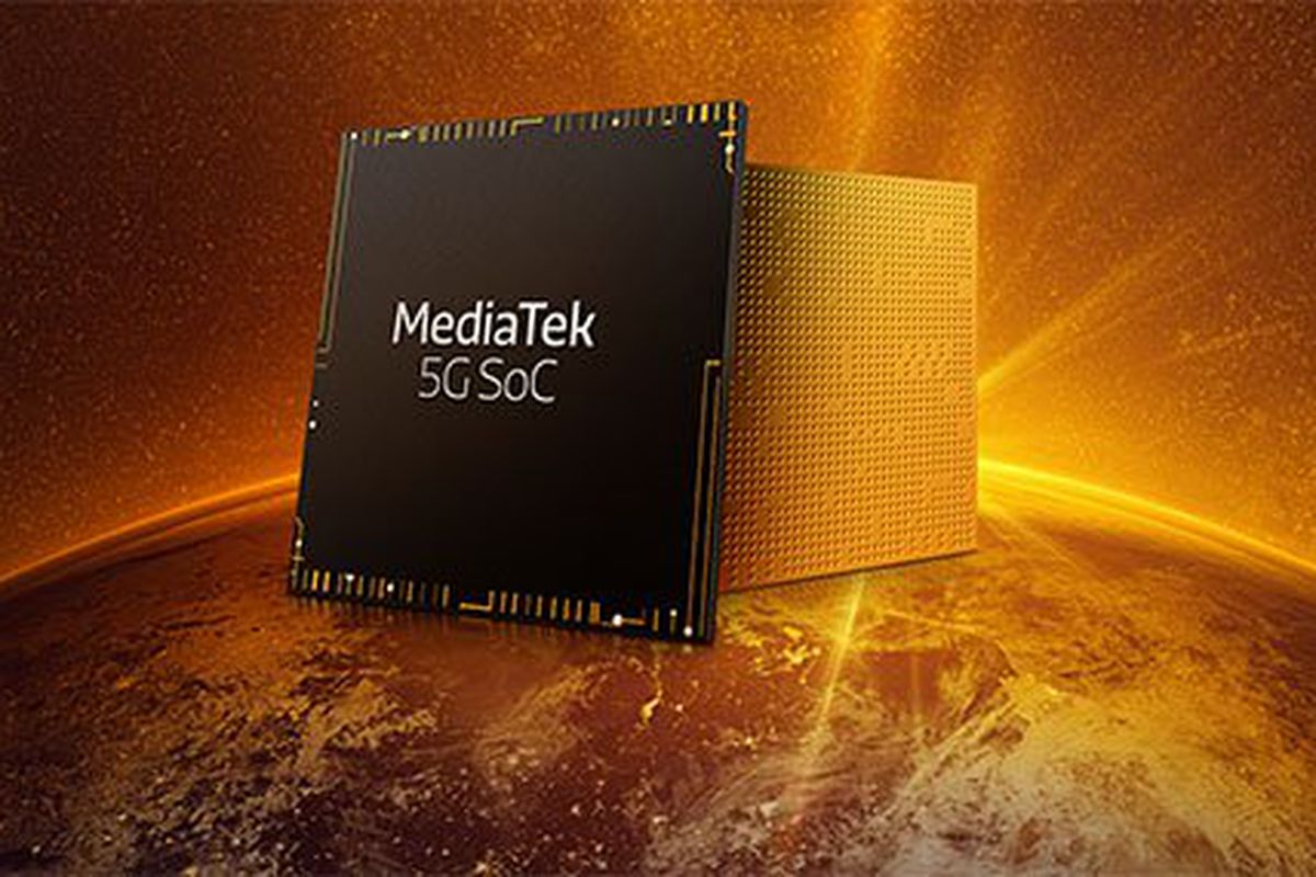
The island holds over 90 percent of global manufacturing capacity for chips at 7 nanometers or below, while more than 30 firms including Taiwan Semiconductor Manufacturing Co and MediaTek Inc formed an industry alliance in 2024.
Silicon photonics replaces conventional copper wiring between chips with optical signals. Because optical transmission generates negligible heat, the technology cuts device power consumption by 30 to 50 percent, according to the Ministry of Economic Affairs. That saving eases cooling limits in high-density AI data centres. It also clears the 1.6-terabit-per-second bandwidth ceiling that hampers electronic links.
Optics Replace Copper Interconnects
Heavy capital is pouring across the hardware supply chain. Nvidia invested US$4 billion into silicon photonics development in March. The chipmaker needs architectures that sustain real-time AI workloads and high-definition streaming without overheating server racks.
Taiwanese authorities have folded the technology into their New 10 Major AI Infrastructure Projects. Funding flows through the government’s A+ Enterprise Innovation research programme. The scheme subsidises domestic research teams and equipment developers building local manufacturing tooling.
Alliance Mobilises Heavyweights
Execution on the ground rests on the Silicon Photonics Industry Alliance, a consortium established in 2024 with industry group SEMI. The group brings together more than 30 technology suppliers. Members include Taiwan Semiconductor Manufacturing Co, ASE Technology Holding, MediaTek and Hon Hai Precision Industry.
Asian hardware vendors and server assemblers face shifting procurement cycles. Traditional printed circuit board layouts will yield to integrated optical packaging. As a result, component suppliers must retool production lines for optical transceivers and precision glass substrates.
Manufacturing risks centre on packaging yields and costs. Integrating laser sources and optical waveguides directly alongside silicon dies requires packaging tolerances tighter than standard wire bonding. These yield hurdles could delay volume delivery.
Race for Next-Generation Packaging
Foundry and packaging operators have spent years researching optics to counter the slowdown of traditional transistor scaling. Physical node shrinking now delivers diminishing returns. Advanced packaging formats like copackaged optics have become the primary path to computing efficiency.
Prototype lines are now running across alliance members to finalise copackaged optics standards before volume production begins for 2026 data centre hardware cycles.