Tag: samsung

  • Samsung adds new models to its Digital Car Key support list, but not all work with UWB

    Samsung adds new models to its Digital Car Key support list, but not all work with UWB

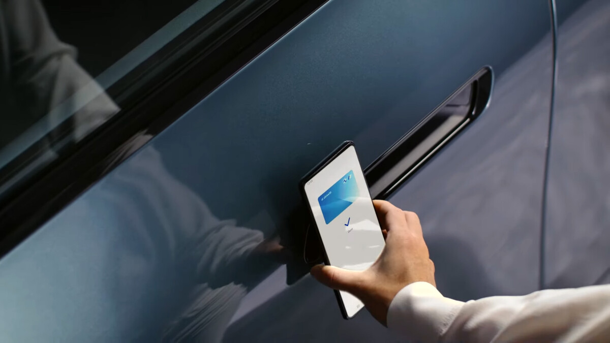
    A few weeks after Apple, the Samsung Digital Car Key initiative announced support for a number of new BMW, Kia, and Genesis models, reports TizenHelp. These include the Genesis GV60, Genesis G90, BMW 1-8 Series, BMW Z4, BMW X5-X7, BMW iX3, BMW iX, BMW i4, and the Kia Niro.

    While the luxury Genesis models will support both NFC and UWB connectivity, the rest only offer NFC support meaning that you will have to hold your Galaxy closer to the car in order to unlock it.
    The feature is available on its home turf for now, but hopefully, Samsung will roll it out for the new car models globally soon, or you can use the digital car key support built into Android 12.
    For now, Samsung’s Digital Car Key option is available only on the Galaxy S22 and S21 series, the oldie Note 20 Ultra, and on Samsung’s foldable phones like the Z Fold 3 and the Z Flip 3. Besides Samsung, Google’s Pixel 6 series are also supporting digital car keys and Google even baked BMW support in Android 12 on a system level.
  • Samsung to introduce recycled parts for smartphone repairs

    Samsung to introduce recycled parts for smartphone repairs

    Samsung is reportedly planning to start a new program that could significantly reduce repair costs for your Galaxy phones.

    Samsung is considering introducing certified recycled parts for mobile repairs. These are parts made of recycled materials such as discarded plastics, metals, and more. The initiative could launch in the next few months, specifically by the first half of this year.

    The report suggests that by using recycled spare parts, Samsung could pass on a smaller repair bill to users. The publication notes that things like display replacement could cost half of what it does today.

    As far as the quality of the recycled repair parts is concerned, Samsung is aiming for a level that can match that of new products. There’s no word on which smartphone parts will be available under the program and how much they would cost exactly.

    Samsung has been promoting sustainable manufacturing for a while now. The Galaxy S22 series is one of the latest examples of its efforts. The phones use a new material made up of discarded fishing nets.

    Over the years, Samsung has also significantly reduced the amount of plastic and paper in its packaging. Recycled repair parts seem to be a logical extension of Samsung’s sustainability efforts.

  • TSMC continues to dominate the global foundry business with Samsung a distant second

    TSMC continues to dominate the global foundry business with Samsung a distant second

    TSMC’s market share during the fourth quarter of last year was 52.1% based on its revenue of $15.7 billion during the three-month period. That was down from the 53.1% share of gross that the foundry had during the previous quarter, but was still well ahead of the next name on the list.

    Behind TSMC was its biggest rival in the industry (at least for now), Samsung Foundry. The latter had 18.3% of industry revenue at the end of the last quarter of 2021. Even with strong 15.3% growth in its top-line on a quarter-over-quarter basis, Samsung’s gross for the period from October through December was only 35% of TSMC’s.

    And things are about to get worse for Samsung. Low yields on the production of some Application Processors (AP) by Samsung, about half the yield rate achieved by TSMC, has led Qualcomm to move over production of some of its most powerful Snapdragon chipsets to TSMC from Samsung. Additionally, Samsung is investigating the disappearance of funds that the foundry unit had supposedly set aside to improve chip production yields.

    Trend Force notes that while Samsung Foundry is showing strong revenue growth, the bottom line has not been able to stay in gear as “the slower ramp-up of advanced process capacity continues to erode overall profitability.”

    TSMC’s results for the quarter were bolstered by strong growth in revenue connected to the production of 5nm chipsets for the iPhone 13 series. The only TSMC process node that showed a drop in the top line for the fourth quarter was the 7nm/6nm unit which was impacted by a weak smartphone market in China. Samsung’s strong 15.3% hike in sequential revenue came about from the completion of its 5nm/4nm advanced process node capacity.

    After the well-known pair of TSMC and Samsung, Taiwan’s United Microelectronics Corporation (UMC) was next as its Q4 revenue comprised 7% of the industry’s revenue for the three months. For the quarter, it garnered $2.12 billion in gross, up 5.8% from its third-quarter revenue. In fourth place, GlobalFoundries kept the 6.1% share of global foundry revenue that it earned during Q3. At number five was China’s largest foundry, SMIC, with a market share of 5.2% and Q4 revenue of $1.58 billion.

    What holds back SMIC is its inability to compete at the current cutting-edge process nodes of 5nm/4nm with both TSMC and Samsung knocking at the door of 3nm. Like the U.S., China is desperately looking to become self-sufficient in semiconductors, and its failure to do so worries experts who fear that China could use TSMC’s success as a reason to take over Taiwan and capture control of the world’s largest contract foundry.

    The industry is far from balanced in terms of revenue with the top five foundries controlling 90% of global foundry market share. That is understandable though when you consider that TSMC and Samsung are the leaders in advanced process nodes.

    The remaining foundries making up 6-10 on the list and their Q4 market shares include HuaHong Group (2.9%), PSMC (2%), VIS (1.5%), Tower (1.4%), and Nexchip (1.2%). The latter might have reported the lowest market share of global foundry revenue for Q4, but it did show the largest growth rate in revenue quarter-over-quarter at 44.2%.

    For the fourth quarter, global foundry revenue came in at $29.55 billion, up 8.3% from the third quarter.

    One of the reasons for TSMC’s success is its long working relationship with Apple. For every $100 in revenue collected by the foundry, $26 comes from Apple. Just last week Apple announced that by combining a pair of its M1 Max SoCs, it created the M1 Ultra which contains a whopping 114 billion transistors inside.
  • Samsung Internet browser adds new privacy and safety features, User Experience improvements

    Samsung Internet browser adds new privacy and safety features, User Experience improvements

    Samsung’s internet browser app is about to get another big update that focuses mainly on security and User Experience improvements. Released as Samsung Internet Beta 17, the most recent app build brings new features that further enhance privacy and safety.

    The highlight of Samsung Internet Beta 17 is Smart Anti Tracking, a privacy and security feature that allows smartphones to automatically remove tracking cookies. Everything is possible thanks to the on-device machine learning, which identifies trackers used by a website and removes them.

    The Smart Anti Tracking feature will be turned on by default in regions like Europe, South Korea and the United States, which means users these parts of the world won’t have to worry about enabling it. The rest of the world can look for the new feature in the setting menu and choose to Always enable it or just when Secret mode is active.

    Furthermore, Samsung Internet Beta 17 make HTTPS scheme the default way to browse websites. Unlike the previous HTTP scheme, HTTPS provides a much safer way to transfer data between the browser and a server.

    Another interest new feature is the addition of a new panel to the Quick Access Page called “privacy board.” This is where you can get an overview of your security and privacy settings for easy access, and it also provide the ability to see Privacy reports.

    More importantly, Samsung Internet Beta 17 introduces “Live Text,” a new feature that allows users to copy, translate or web search on text within an image on the internet. To do that, you just have to long press on an image in the web page and a new Live Text UI should pop up to let you choose what you want to do.

    Along with these new features that focus on privacy and safety for the most part, Samsung has included a bunch of UX enhancements. Here are the most important ones:

    • Bottom URL bar: When tapping the URL bar using the ‘bottom layout’, the URL bar will be shown directly above the keyboard when editing. All the basic functions and interactions are the same as the top layout.
    • Shortcut to move to Customize menu: Move to Customize menu when long pressing on any button of Tools menu to make it easier to edit items
    • Drag and Drop in Bookmark: Provides Drag and drop to move bookmark item in the Bookmark bar
    • Video subtitle position enhancement: Subtitle position enhancement of Subtitle extension for Fullscreen video.

    Samsung Internet Beta 17 is available as a separate download via the Galaxy Store. If you don’t feel like testing a non-final version of the software would be a good idea, you can definitely wait for the stable version to come out in the just a few weeks (hopefully).

  • Samsung Pay’s security receives a “very good” test rating

    Samsung Pay’s security receives a “very good” test rating

    Samsung Pay’s security is in the “very good” category. This was announced by the tech giant in an official newsroom post. According to the post, Samsung Pay scored 450 points out of 500 in a security test conducted by an independent agency called umlaut. Umlaut is part of the Ireland-based IT company Accenture and offers ‘advisory and engineering services to clients all over the world.’

    In its post, Samsung stated that Samsung Pay meets the requirements of umlaut’s test procedure in ‘all tested aspects.’ During the security test, Samsung Pay was tested in four areas:

    • security of data traffic between smartphone and bank
    • compliance with secure programming standards
    • data protection on the smartphone
    • protection against malicious attacks by third parties.

    In the “security of data traffic” tests, testers inspected the types of security algorithms and protocols implemented into Samsung Pay. They also examined how sensitive data is transmitted and if the app has the appropriate measures in place to protect its users from man-in-the-middle attacks, which control and manipulate data traffic.

    In the “compliance with secure programming standards” test, the testers from umlaut checked if Samsung Pay uses secure programming methods and if there is any hidden sensitive information in the app’s source code. During the “checking data protection” tests, the experts tested how securely the Samsung Pay app stores sensitive data and if this data is protected from third parties. The app was also tested against impersonation attacks. These are attacks where the user was tricked into using Samsung Pay on fake apps or websites.

    In regard to Samsung Pay’s good test results, Gerrit Povel, Vice President, Direct to Consumer Division at Samsung Germany, stated, “We play it safe with mobile payment. The result of the independent test by umlaut proves the high priority that security has in the development and operation of the Samsung Pay app. The rating ‘very good’ underlines the role of Samsung Pay as a leading solution in mobile payment.”

  • Samsung allegedly fell victim to a data breach

    Samsung allegedly fell victim to a data breach

    There has been a new security breach in the tech industry. This time, the victim was reportedly Samsung Electronics. The hackers taking responsibility for the data breach are from the Lapsus$ hacking group. Lapsus$ has leaked around 190GB of what it claims to be confidential data from Samsung, which includes source code and biometric unlocking algorithms.

    As proof of the data breach, Lapsus$ has also provided a screenshot of C/C++ code directives, alleging that they came from Samsung. In a description of the 190GB of stolen data the hacking group teased before the big leak, they wrote that these 190GB contain “confidential Samsung source code” and listed exactly what the hacking group managed to steal from Samsung.

    With its hack, Lapsus$ got its hands on the source code for every Trusted Applet (TA) installed in Samsung’s TrustZone. Samsung TrustZone is a secure environment utilized for operations such as hardware cryptography, binary encryption, and access control.

    Lapsus$ also managed to steal algorithms for all biometric unlock operations, the source code used for booting all recent Samsung devices, and confidential source code allegedly originating from Qualcomm. With its attack, Lapsus$ also stole the source code for Samsung’s activation servers, аs well as that used for authorizing and authenticating Samsung accounts, including APIs and services.

    Although the information above is what Lapsus$ listed as the stolen data, it is unknown if Lapsus$ stole additional secret information from Samsung. What is known, however, is that the hacking group has split the leaked data into three compressed files and made it available for download via a torrent.

    As for a comment from Samsung about the data breach, Samsung officials told the media outlet that they ‘are now assessing the situation.’

  • Samsung Electronics CEO accepts unions’ request for talks

    Samsung Electronics CEO accepts unions’ request for talks

    The past few weeks have been a rather turbulent time for Samsung Electronics, and it had nothing to do with the Galaxy S22 series. The company has been heading towards its potential first-ever strike, with a workers’ union coming together to fight against unfairly low wages—but Samsung has already taken the first move towards remedying the situation.

    The workers’ union at Samsung had submitted a demand for wage renegotiations which was to be answered by Friday at the latest, to avoid a full-blown strike. The union was already legally authorized to go on strike, but on Friday, the company committed to an official meeting for wage negotiations to be held in early March.

    The employees involved in the union had been growing increasingly dissatisfied at the company’s refusal to provide significant wage increases or bonuses after the company’s performance in 2021. Although Samsung reportedly fell short of its 2021 production goals, this was owed to the devastation of the pandemic and chip shortages, rather than any drop in employee performance.

    Earlier this month, the union requested that the workers be granted a ten-million-won (roughly $8,400) annual salary increase, as well as performance-based bonuses calculated at 25% of the year’s operating profit.

    The company originally blatantly rejected the demand, but thanks to Samsung’s response on Friday, however, a full strike may be avoided if the two parties come to a mutually satisfactory agreement.

    The organizers of the union stated on Friday that “We received an official reply from the management to our request for a dialogue with the company’s chief executives. We are delighted that the management has changed its stance.”Because of the size of the company, Samsung still hasn’t been decided which CEO will be chosen to participate in the discussion. The upcoming CEO election may complicate the factors around the decision, as the election will take place on March 16, where President Kyung Kye-hyun will be appointed as a new co-CEO.

  • Samsung execs accused of doctoring 5nm chip yield results to hide stolen funds

    Samsung execs accused of doctoring 5nm chip yield results to hide stolen funds

    On the heels of a report claiming that Qualcomm is so upset about the low 35% yield achieved by Samsung Foundry’s 4nm process node that it dumped Sammy for TSMC, another alarming report has surfaced. Samsung is investigating the possibility that fraud occurred inside the company’s foundry business.

    Unnamed Samsung Foundry executives are being accused in the Korean media of fabricating the yield rate data achieved by Samsung Foundry for its 4nm and 5nm process node. This data, expressed as a percentage, shows how many chips in a wafer meet quality testing standards. Yesterday’s report indicated that the yield for Samsung Foundry’s 4nm process node was a poor 35% compared to the 70% yield achieved by rival TSMC.

    The poor yield was mentioned in a report as the reason why Qualcomm supposedly replaced Samsung Foundry with TSMC for the production of next year’s Snapdragon 8 Gen 2 Application Processor. The new report claims that the 4nm and 5nm yields were faked by Samsung Foundry executives to make it seem that everything was going well with the division.

    Samsung officials are trying to track down funds that were supposed to be used to improve the yield at Samsung Foundry. Reports of the poor yields and missing funds at Samsung Foundry come at a poor time for Samsung since it and TSMC are the only two foundries in the world able of churning out chips at a process node of under 5nm. Both are working hard to become the first foundry able to ship 3nm components.

    TSMC already has plenty of business as its customer list includes heavyweights such as Apple, MediaTek, Nvidia, and more. TSMC is believed to be running into yield problems of its own at the 3nm process node although volume production is only supposed to be reached later this year.

    The lower the process node, the higher the number of transistors that can fit in a chip. That is key to the performance of the component since the more transistors used, the more powerful and energy-efficient a chip is.

    A Samsung official familiar with the situation said in a quote translated by Machine Learning, “Since the delivered quantities is struggled to meet the recent foundry order volume, we have doubts about the yield of the non-memory process, which has was known to be achieved.”

    The official added, “The management consulting investigates the claims on the yield of a semiconductor foundry by former and current DS division executives. The consulting will determine whether the claims are false.”

    If this story sounds strange and bizarre, that’s because it is. Frankly, we can’t think of a story that is similar to this one. And that means that until more official statements are issued by Samsung or even the police in Korea, we should take this report with a grain of salt.

Samsung’s foundry business set a company record for revenue during the fourth quarter of 2021. On a sequential basis, profits declined from the third quarter of last year as Samsung had to spend more money to ramp up advanced process nodes such as 4nm and 3nm. Whether some of that money has to do with the funds allegedly missing is not clear.

The increase in revenue to a record high in the foundry business came from increased sales to HPC (High Performance Computing) customers. For the current quarter, the first quarter of 2022, Samsung said that its foundry would “focus on improving its advanced process yield to improve its supply stability. Also, the Company will continue technical leadership through mass production of the 1st generation GAA process in the first half of 2022.”

GAA, or Gate All Around, is a transistor structure associated with Samsung’s 3nm process node. It replaces (for Samsung, anyway) the FinFET structure used presently.

Samsung Foundry says that the chip market will remain “tight” as 5G penetrates more market, and demand from High Performance Computing firms remains solid. Additionally, the need for manufacturers to have more chips than needed just in case there is a supply shock from an external event, and outsourcing demand from integrated device manufacturers (ISDMs) who design and build their own chips (like Intel) will keep the assembly lines humming in 2022.

For this year, Samsung expects supply to remain tight due to rising penetration of 5G, solid HPC demand, growing out-sourcing from IDM players and continued needs for securing safety inventory. The Company aims to exceed market growth by expanding capacity at advanced nodes, adjusting prices and adding new customers.

  • Samsung invests another $920 mln in northern plant

    Samsung invests another $920 mln in northern plant

    Samsung has received permission to invest an additional $920 million in its electronic components plant in the northern province of Thai Nguyen.

    The license, awarded to the South Korean’s electronics giant’s Samsung Electro-Mechanics unit, will increase its total registered investment in the province by 68 percent to $2.27 billion.

    Samsung, Vietnam’s biggest foreign direct investor, first invested $1.3 billion in the electro-mechanics unit in 2013. The unit produces mainboards and other electronics components.

    As of last year, Samsung had invested $18 billion in Vietnam. It has six plants in the country and is building a new research and development center in Hanoi.

  • Samsung invests another $920 mln in northern plant

    Samsung invests another $920 mln in northern plant

    Samsung has received permission to invest an additional $920 million in its electronic components plant in the northern province of Thai Nguyen.

    The license, awarded to the South Korean’s electronics giant’s Samsung Electro-Mechanics unit, will increase its total registered investment in the province by 68 percent to $2.27 billion.

    Samsung, Vietnam’s biggest foreign direct investor, first invested $1.3 billion in the electro-mechanics unit in 2013. The unit produces main boards and other electronics components.

    As of last year, Samsung had invested $18 billion in Vietnam. It has six plants in the country and is building a new research and development center in Hanoi.

  • Over 90 pct of Samsung, Intel workers return to work after Tet

    Over 90 pct of Samsung, Intel workers return to work after Tet

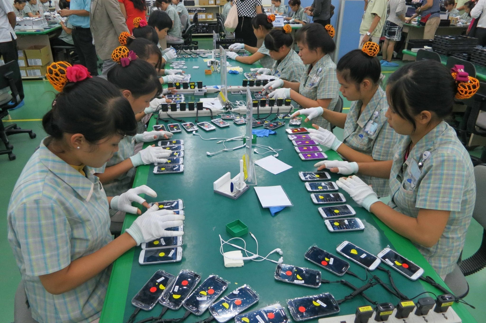
    Major factories in Ho Chi Minh City reported over 90 percent of employees returning to work after the nine-day Tet holiday, abating employer concerns of a labor shortage.

    Some factories with high return rates are Samsung electronics manufacturer HCMC CE Complex (95 percent) and motor parts maker Nidec Sankyo (94 percent). Other manufacturers like Intel and Jabil also reported a return rate of over 90 percent.

    Eight factories in Saigon Hi-tech Park of Thu Duc City, which utilize over 45,000 employees, reported between 80 percent and 95 percent of workers returning to work Tuesday after the annual Lunar New Year’s holiday Tet, according to park data.

    Over 17 industrial zones and manufacturing areas where 273,000 employees work posted a return of 82 percent.

    The high return rate is considered a relief to HCMC employers who, before the holiday, had expected a shortage of workers after Tet as many preferred to stay in their hometown.

    Tet, Vietnam’s biggest national holiday, is a time when workers of large industrial parks leave en masse for their hometowns for family renuions.

    Some factories of Vinatex, one of the biggest garment companies in Vietnam, posted a worker return rate of 100 percent as the company started off the year three days before the holiday ended to meet the surge in order numbers.

    Pou Yuen, footwear maker and biggest employer in HCMC, is expected to see its return ratio rising from 64 percent Monday to 90 percent Wednesday.

  • Soon we may be using more secure payment cards thanks to Samsung

    Soon we may be using more secure payment cards thanks to Samsung

    Samsung has announced the S3B512C security chip, its new fingerprint security chip developed in partnership with Mastercard, designed primarily for payment cards. According to the company, the chip is the ‘industry’s first all-in-one security chip solution’ and would be able to provide faster and safer interactions while making purchases. Because Samsung’s chip uses biometric authentication, the chip would also remove the need to enter your PIN code on a keypad.

    The S3B512C chip has a fingerprint sensor as well as a tamper-proof secure element (SE) that meets international security requirements, and a secure processor. The chip captures the user’s biometric data via its fingerprint sensor. Then, using the SE, it stores and authenticates the received information. After that, the chip analyzes the data by using its secure processor.

    With its biometric authentication, Samsung’s security chip may prevent fraudulent transactions which could otherwise be made with lost or stolen traditional cards. Because it has securely saved the owner’s fingerprint, a card using Samsung’s chip will check if the person performing the transaction is indeed the rightful owner. The chip also utilizes anti-spoofing technology, which prevents unauthorized users from fooling the security system using tactics such as artificial fingerprints.

    According to Samsung, although the S3B512C chip is primarily designed for payment cards, it could also be used in cards intended for highly secure authentication, such as student or employee access cards. In addition, by utilizing a fingerprint sensor, a tamper-proof secure element, and a secure processor, the S3B512C may assist card makers in reducing the number of required chips in manufacturing biometric payment cards and might help optimize card design processes.

    Although Samsung’s new security chip sounds very promising, currently, there is no information on when Mastercard will implement Samsung’s new chip.

    Currently, Mastercard offers fingerprint-authenticated payment cards, but they are not as secure as the new Samsung chip and don’t use anti-spoofing technology.

  • Samsung is first in the world to invent MRAM in-memory computing

    Samsung is first in the world to invent MRAM in-memory computing

    Samsung has long been at the forefront of tech innovation, both when it comes to mobile technology and other electronics. The Korean giant just re-affirmed that fact this week, when they became the first company in the world to demonstrate a working in-memory computing process on MRAM.

    In devices like smartphones and computers, most of the computing processes are performed by the processing chip, which exists just for this purpose and is highly efficient at it—despite additionally being one of the most power-hungry components.

    A device’s memory (or RAM) on the other hand, bears the traditional purpose of temporarily storing bits of information for the processor to access immediately, anytime it asks for it.

    This memory allows for much faster data transfer with the processor than a storage drive, but also comes in much smaller quantities—such as 4GB, 6GB, or 8GB or 16GB depending on your traditional computing device.

    For years now, however, there has been plenty of experimentation with the quest to come up with an efficient and practical in-memory computing solution.

    While many other solutions have already been found using alternative types of RAM (such as PRAM or RRAM), as SamMobile notes, MRAM in-memory computing had not yet been prototyped in working form. At least until now, when Samsung has finally managed to create the first prototype.

    Most of the computing devices we interact with from day to day—namely smartphones and computers—run with DRAM, or Dynamic Random Access Memory, as their main memory.

    This type of memory is dynamic and volatile, meaning it only stores information as long as the device is powered on with a current flowing through, and it needs to be constantly refreshed or overwritten in order to retain that data.

    MRAM, on the other hand—Magnetoresistive Random Access Memory—is a type of non-volatile memory, meaning it can retain bits of data even without an electric current flowing through. It stores memory on magnetic charges, rather than electric charges like standard RAM.

    MRAM’s main advantage is its extremely low power usage, although it has faced difficulties in practical integration in modern everyday technology, such as keeping write error rates adequately low. It is also more hostile to in-memory computing than DRAM because of its low resistance.

    Samsung’s in-house MRAM, built for the first computer to ever use it as its main memory

    The main appeal of in-memory computing as a rule, is that it allows for substantial savings of both time and power. A system that performs at least part of its computing inside the memory, will end up saving all of those milliseconds which it would otherwise take for that data to be requested by the processor, travel to the processor, and be processed there.

    Memory also takes significantly less power than a processing chip—which is responsible for a whole slew of tasks at any given time—which is why a device using in-memory computing will also save on energy.

    Samsung believes that once further developed, MRAM technology will truly shine in processing tasks for artificial intelligence. When tested in AI applications, Samsung demonstrated that its in-memory computing process produced a 93% success rate in picking out specific faces in images, and 98% accuracy in its ability to recognize handwritten numbers.

    One of the main authors of Samsung’s research paper, Dr. Seungchul Jung, made the following statement:

    “In-memory computing draws similarity to the brain in the sense that in the brain, computing also occurs within the network of biological memories, or synapses, the points where neurons touch one another. In fact, while the computing performed by our MRAM network for now has a different purpose from the computing performed by the brain, such solid-state memory network may in the future be used as a platform to mimic the brain by modeling the brain’s synapse connectivity.”

    Samsung hopes that this new invention will be revolutionary in increasing the power efficiency in AI chips more than was ever considered possible before.

  • Exynos 2200 finally has a reveal date

    Exynos 2200 finally has a reveal date

    Samsung has finally announced a date for the reveal of the in-house Exynos 2200 chip that will likely power the Galaxy S22 series.

    Samsung and AMD have been working on a GPU for quite some time and it will be integrated into the South Korean giant’s next flagship chip. According to a new rumor, the GPU itself will be called the Xclipse 920.

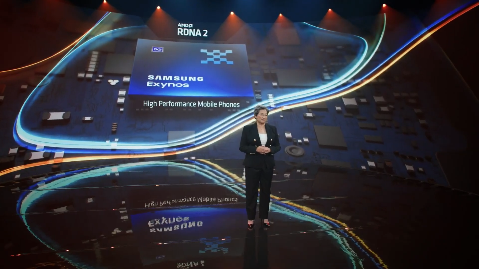
    The company has confirmed that the RDNA 2-powered chip will be unveiled on January 11, which is also when the Galaxy S21 FE is rumored to go on sale.

    Samsung has steadily been upping its chip game. Last year, it embraced Arm’s CPU designs, and now, the AMD-made GPU will take care of the graphics. Whether the new Exynos chip will live up to the hype is a whole different question.

    Qualcomm claims that its new chip offers 20 percent faster CPU capabilities and 30 percent better graphics when compared to the Snapdragon 888. Although the Exynos 2200 is expected to have the same core architecture as the Snapdragon 8 Gen 1 which will fuel the American variants of the Galaxy S22, it may lag behind in performance.

    Per a recent leak, Samsung’s new SoC will offer a 5 percent improvement in CPU performance and a 17 percent increase in graphics when compared to the Exynos 2100 that powers the Galaxy S21 range. That’s not necessarily a cause for concern, because the same leak says that artificial intelligence performance will improve by a staggering 117 percent.

    Although today’s premium phones are plenty fast already, we are still curious to see how the Exynos 2200 will stack up against the flagship chips that power the top phones of 2021. Samsung will allegedly announce the Galaxy S22 series in February.

  • Microsoft to partner with Samsung over HoloLens 3 development

    Microsoft to partner with Samsung over HoloLens 3 development

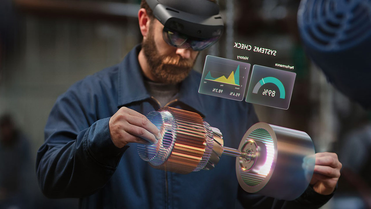
    This summer, Samsung has apparently entered into a partnership with Microsoft over its HoloLens augmented reality project, and the two companies are expected to work on the next generation of the VR headgear for at least two years.

    Microsoft already has a strong partnership with Samsung over preinstalled Office Mobile and other apps on the handsets of the world’s largest phone maker, so taking advantage of its hardware expertise could only be beneficial, too.

    Back in March, Samsung reportedly assembled a task force to probe the viability of the HoloLens partnership, involving multiple departments and has subsequently been given the green light to take on the challenge to be Microsoft’s AT/VR gear maker.

    Commercialization of Microsoft’s HoloLens wearable that takes advantage of Samsung’s engineering prowess will happen after the end of the development contract, in 2024, report the insiders. Samsung’s purchase of AR company DigiLens, along with its display expertise may be what prompted Microsoft to partner with it over the next HoloLens endeavor.

    DigiLens was known for its waveguide technology “used to bend the light from the video playing on a display to the glasses, which is transparent in AR display devices as users need to see the real surrounding around them simultaneously with the virtual items on display.”

    This strongly suggests that the HoloLens 3 may be conceived as a direct answer to the purported Apple Glasses AR/VR headset which is expected to land as soon as next year. Microsoft sold about 200,000 HoloLens 2 devices this year, and it will have to pour a lot of resources to make the third edition stand out as not only Apple, but also Facebook’s Meta, are expected to release their own augmented reality contraptions very soon.